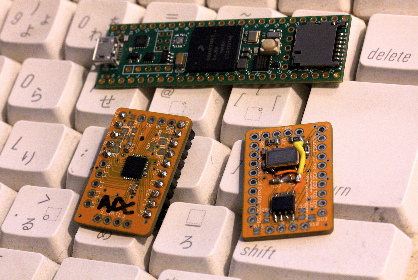
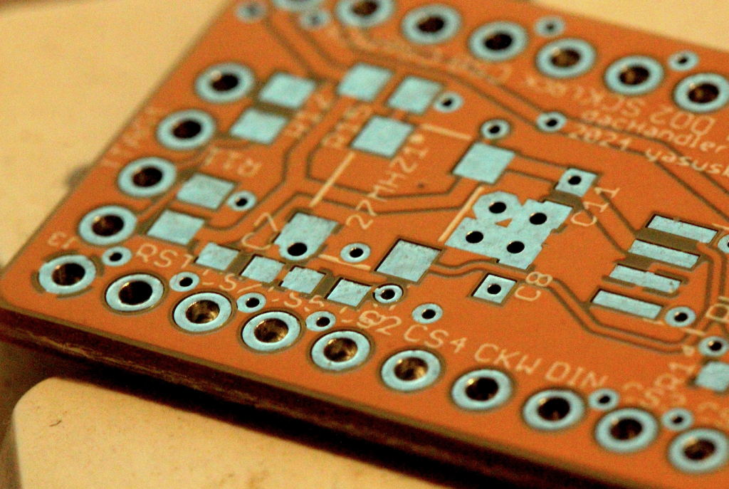
It’s been a while since I assembled a piggyback FPGA board, but I had to deal with a short circuit on a terminal caused by a TCXO installation error.
The short-circuit occurred on the GND / OscOut side land, where a jumper plug was used to repair a printed pattern that was damaged when pulling off the TCXO that was suspected to be faulty. Yellow is VCC and orange is 27MHz clock line connected.
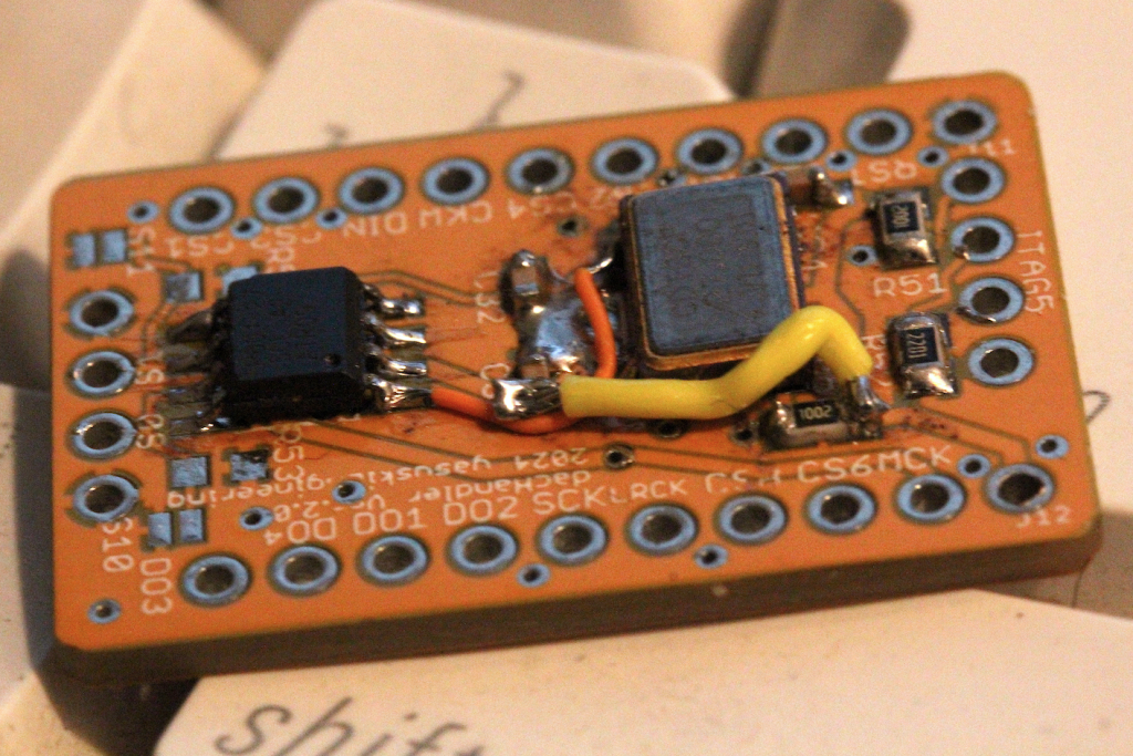
It should be noted that hand mounting of TCXOs is highly challenging and failure to do so can induce serious problems such as “short-circuiting the power supply” in the worst case.
The symptom that the adjacent VCC land TCXO’s OscOut land is short-circuited by solder bridge is obviously my design error, so it would be correct to try a more reliable method of component mounting, such as a reflow method using a used oven or iron.
I measured the resistance value to confirm the repair of the power supply line, and found that it is more advantageous in terms of power supply efficiency to use jumper-arranged lines to supply power to the FPGA rather than thin printed wiring. If you cannot handle a 4-layer board, it is one way of thinking to deal with such an allowance even if it takes a lot of time and effort.
Addendum:
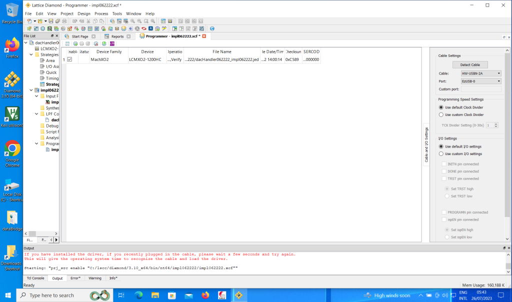
I was able to write the Firmware to the modified base without trouble.

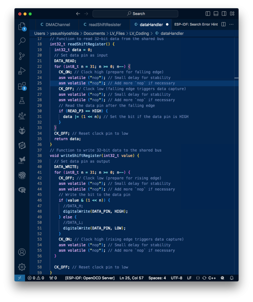
Now I am ready to experiment with high speed serial audio stream using FPGA in the configuration of adc → mcu1 → bus → mcu2 → dac.