I have started designing adcHandler.
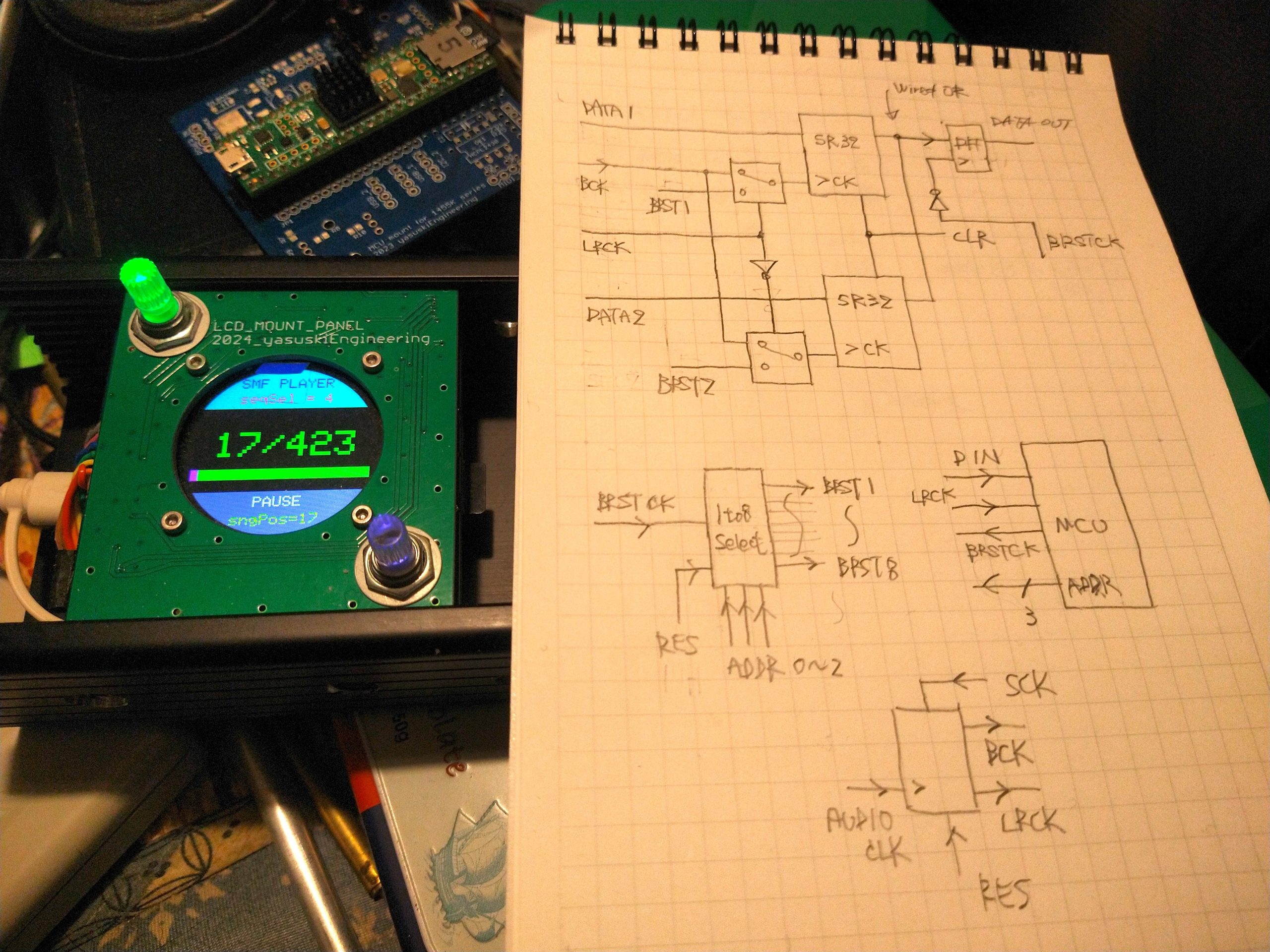
In the process of drawing a block diagram on my notebook to summarize the overall structure, I came up with a device that uses a 2-wire + channel CS configuration for high-speed communication.
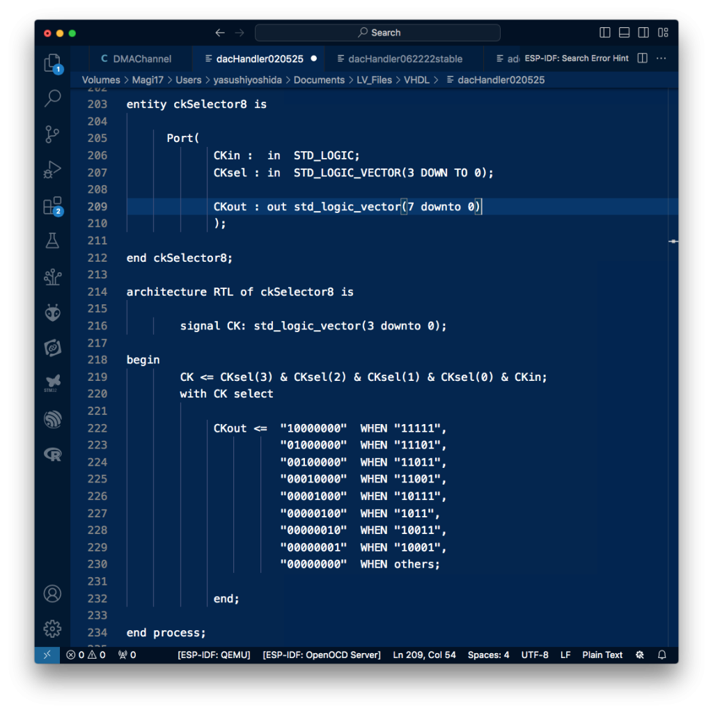
In order to slim down the terminals, I came up with the idea of constructing a circuit with INH + chAddress, and tried to describe the selector using vectors, but I completely forgot the VHDL syntax.
In order to dig up my memory, I unearthed a special book on tiger techniques from the archives and checked the basic syntax, but the 20-year-old material seemed old-fashioned, and in fact, the VHDL specification was revised around 2008.
For example, a function called reduce_or had been added, so I tentatively tried to build a Wired OR using it, but the results of the experiment were negative, and unfortunately it turned out that Lattice’s IDE did not implement this function, so I had to use the old orthodox method for the design. The design was to be performed using the old orthodox method.
First, I wrote a selector to consolidate ChipSelect, which used to be distributed to each clock line controlling 32-bit shift registers, into one place.
The attempt this time is to rationalize the CS lines, which used to have 8 lines but are now reduced to 4 lines. On the other hand, on the MCU side, the steps required for addressing are added, so a slight degradation in processing capacity is expected.
The structure of adcHandler is the opposite of that of dacHandler. I wasn’t sure about the way to specify the pins, such as orIn(0), which I did for the device that imitates WiredOR, which summarizes the final output stage, but it seems to have been accepted.

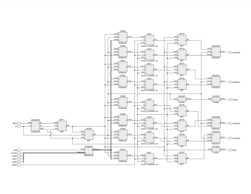
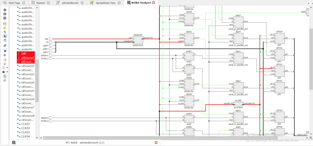
The overall structure of the newly assembled adcHandler looks like this.
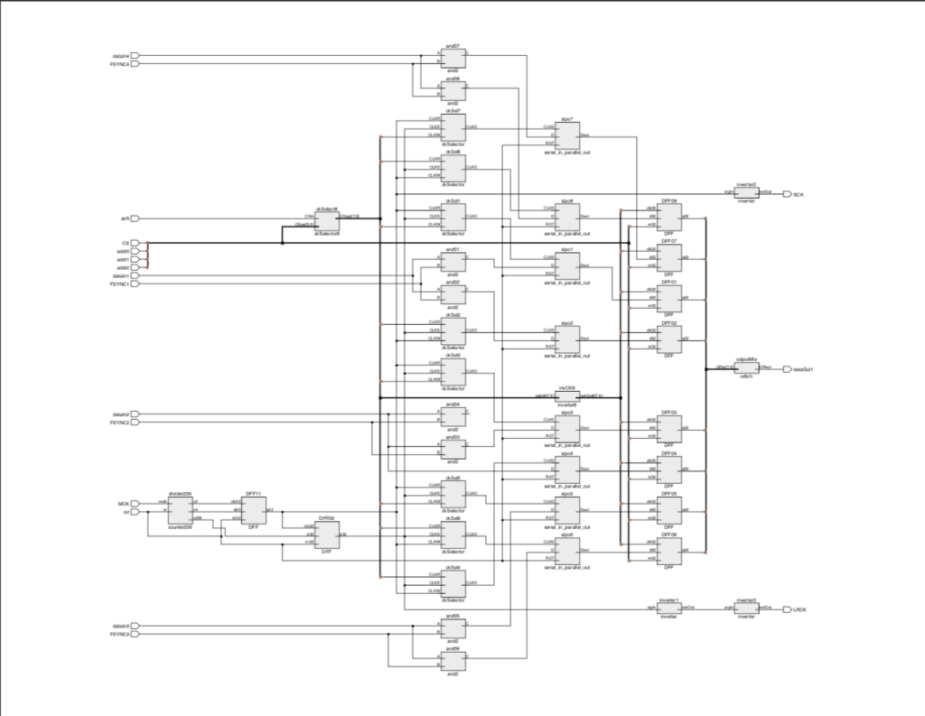
To handle the data output from adc, an internal signal line was added.

The LRCK signal line, which oversees the data line exchange, retains its conventional style.
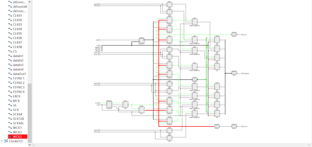
Similarly, the SCK routing is unchanged, but in any case, there may be a polarity mismatch.
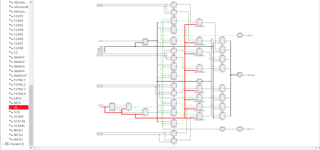
As for the reset circuit, the D-FF before the end stage has been removed from the wiring.
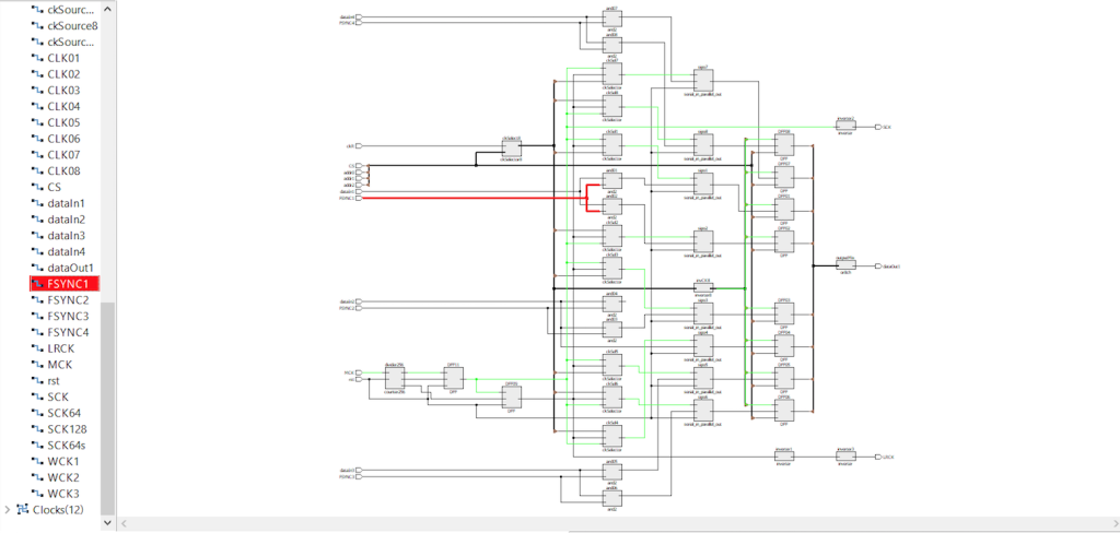
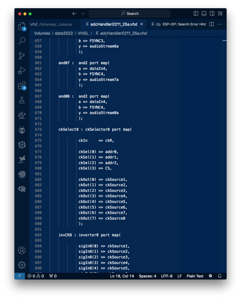
I added 4 FSYNC input pins to mask the LSB data from the 24-bit precision ADC that is supposed to be used in this project.
The D-FF before the final stage is reset at the timing when a “L” is input from the CS pin.
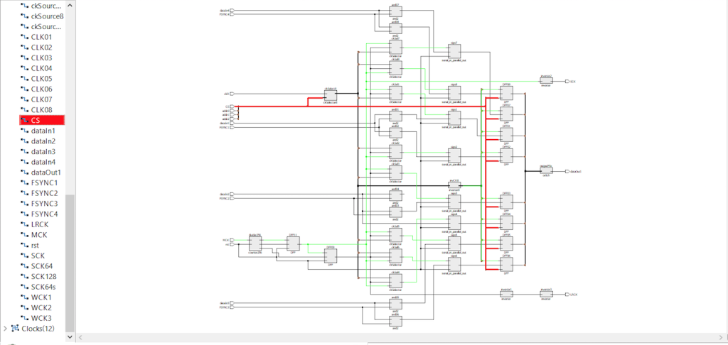
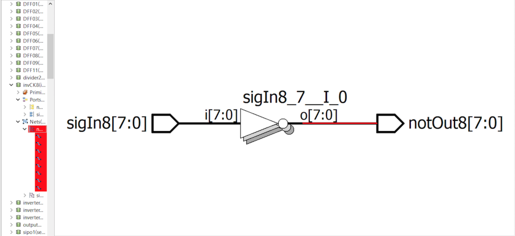
The D-FF clock line is inverted by the Inverter.
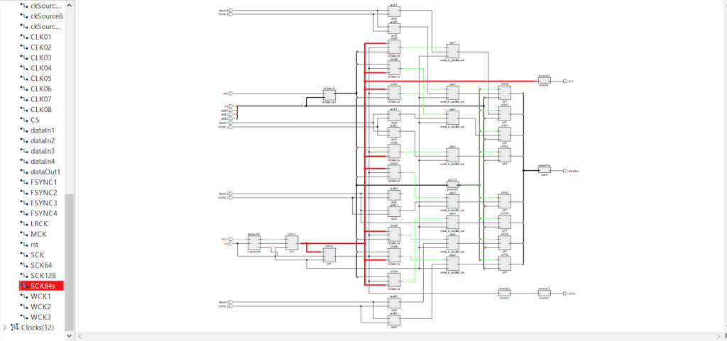
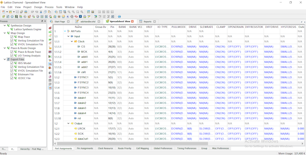
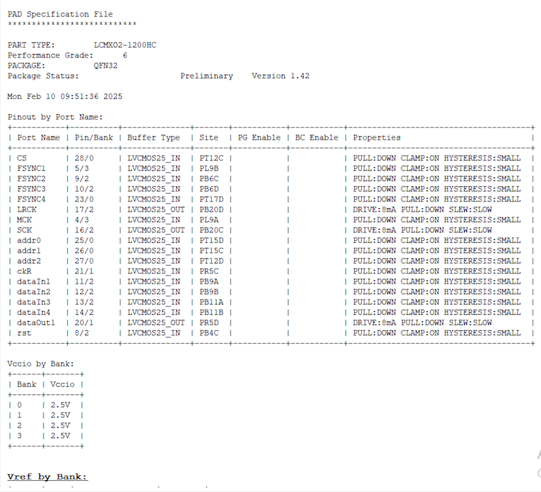
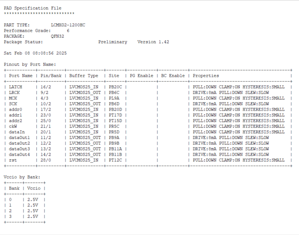
The pins are arranged like this.
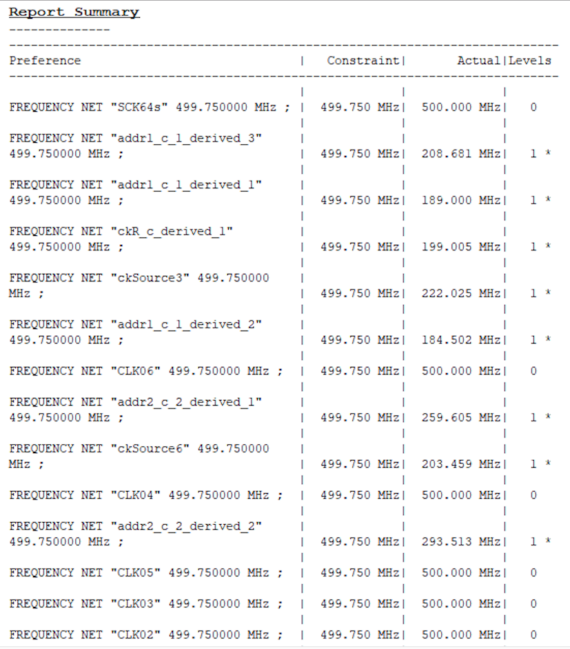
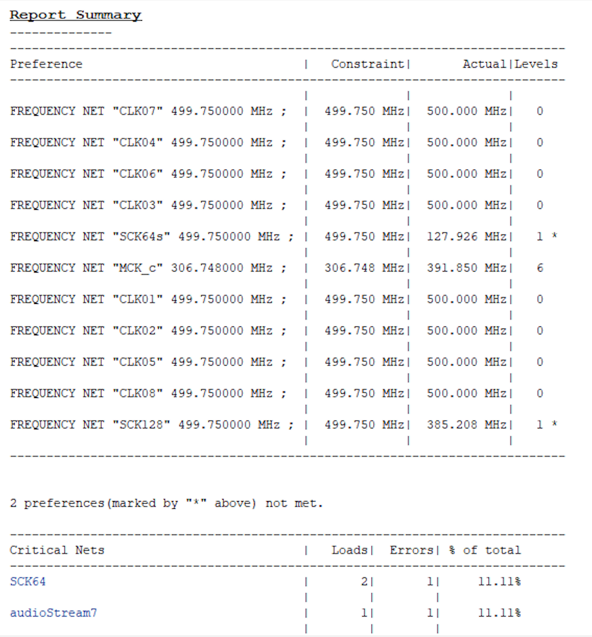
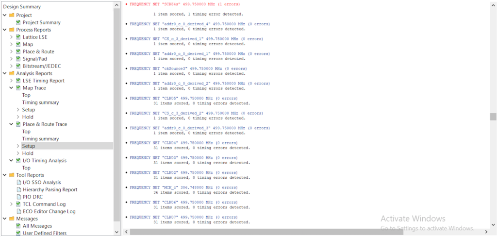
The red alert indicates an error, but the error is recovered immediately, so there should be no problem. The bottleneck in processing speed seems to be within an acceptable range.
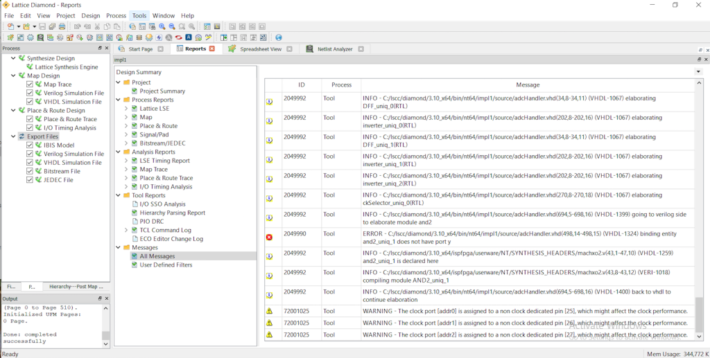
Since the timing of releasing the accumulated data is critical, we have to experiment to find the problem, but we have not confirmed the “warning of serious delay” that appeared with the old dacHandler.
I decided to update the dacHandler while I rearranged the clock lines around the shift register.
The pin layout of the old dacHandler had a full channel configuration of D/CLK/CS*8. The new design consumes almost half as many pins, 6 in total, D/CLK/addr0~2/C.

In this case, the number of output pins required on the MCU side will be reduced from 6 pins (D/CLK/CS*4) to 5 pins (D/CLK/addr0~1/CS).
The speed seems to be secured here as well,
There seems to be almost no serious limitation.
Addendum (0211_25):
By modifying the configuration of the sequential processing area,
I may be able to recover most of the errors that were occurring in some places while reducing the delay of data lines.
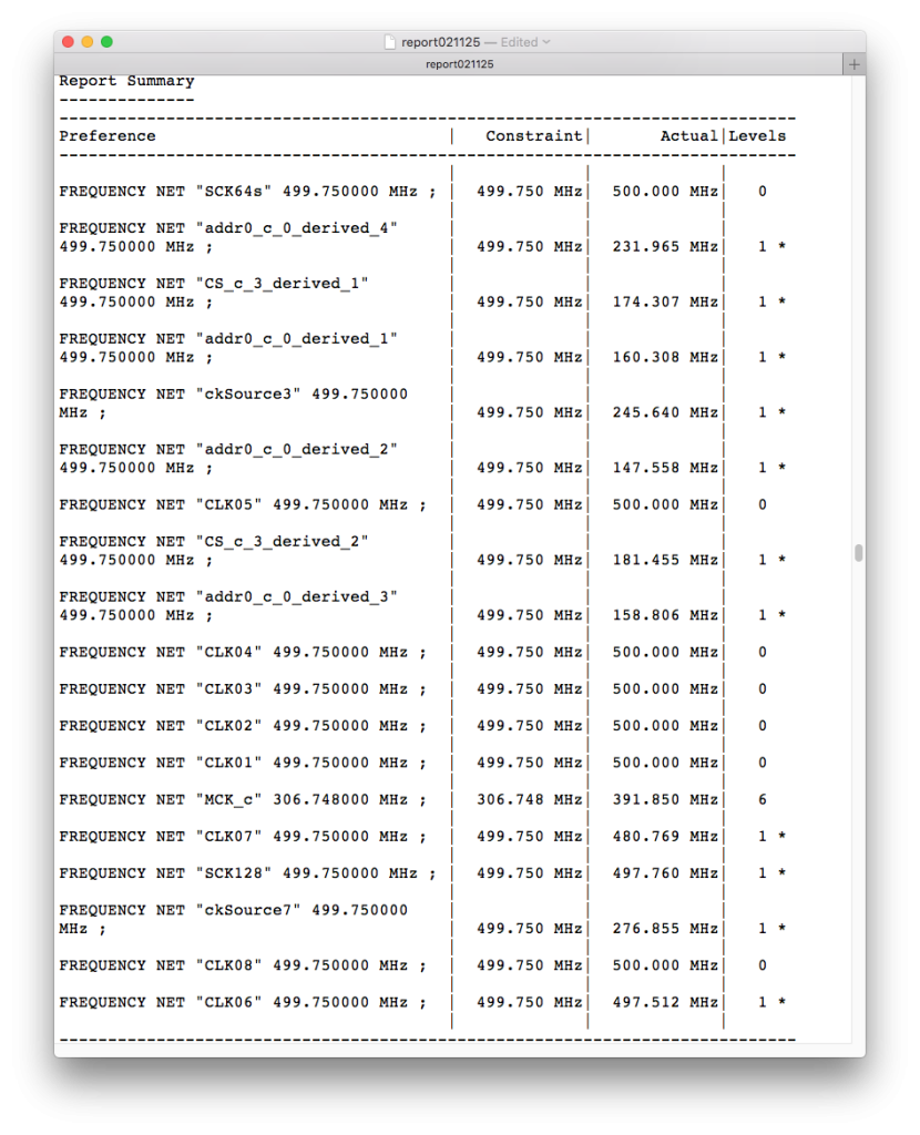
The AnalysisReport error report is as follows
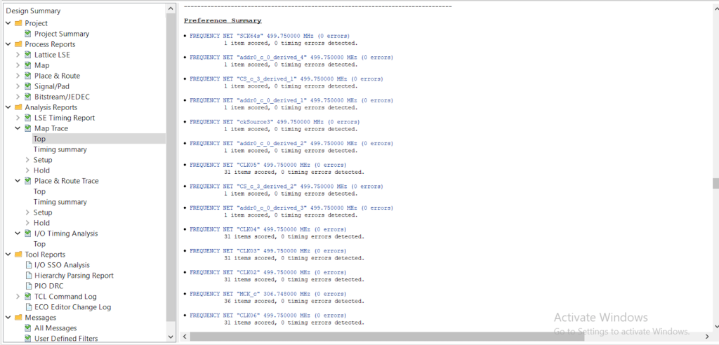
It appears that the error that occurred on the signal line, which requires high-speed operation, has been resolved.
Place & RouteTrace error report.
Except for the two lines that divided MCK, the error appears to have been addressed.
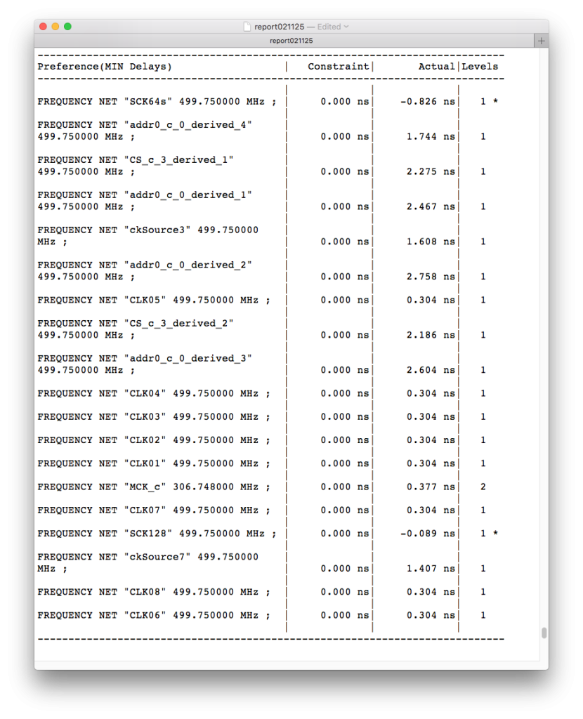
The clock line bottleneck is 245MHz, so things are looking up.